CS 220 - Lab 5: Designing a Complete CPU (Onion Soup!)
Due 5:00pm October 31
General Lab Goals
This lab provides an opportunity to design the fetch/execute cycle of a
complete CPU and then implement the CPU by defining circuits for its
control functions and combining it with the ALU and memory you designed
in earlier labs. This project is based on a new machine architecture
called MINIJVM, which is a subset of the Integer Java Virtual Machine
(IJVM) introduced
in Chapter 4. Unlike the IJVM, the MINIJVM's simplicity allows us
to
implement it in LogicWorks. The on-line document Design of a Complete CPU and Memory System
describes this new machine in more detail, along with an example
of programming at this level of architecture.
Because this is an ambitious project, the following teams will reunite
to complete it.
Team Members
A
Phillippe, Vic, Elliott
B Brendan, Henry, Christine
Summary of tasks to be completed by each team:
1. Exercise the complete CPU designed by last year's CS220 class.
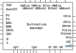
2. Design the circuits for each of the pins on the Instruction
Decoder.
3. Implement the Instruction Decoder.
4. Turn in the items described in Part 4.
Part 1: Exercise the Complete CPU
Drag the file MINIJVMFINAL.cct
to the desktop, start up LogicWorks, and open this file. It
should look like the circuit attached to this lab (Ugh!).
Now set the simulator at about half speed - you should see red lines in
the A, B, and D buses and a blue line in the C bus. Now turn off
and on the switch labeled ON at the top of the circuit - this starts
the machine running. You should see a timing chart that looks like the
one on the attached sheet, which shows the first 8-10 clock cycles when
running a bytecode program.
The program that is running is the one that appears at the end of the
document Design
of a Complete
CPU and Memory System, which calculates the factorial of
n. If you let it run to completion, the result will be stored in
memory location 32 (the variable f).
Before moving to Part 2, answer the following questions:
- When this machine begins running, the PC is loaded with 00 and
the SP is loaded with 80 (an empty stack). Why?
- The A and D buses are paired, in the sense that a memory read or
write will require the A bus to carry the address of the byte read/written
and the D bus carries the value
of that byte. Look at the attached timing chart. When the
clock rises at about time 500, how do you interpret the fact that Bus
A=00 and Bus D=10?
- Write down all the control switches (PCin, MDRin, F0, F1, etc.)
that are set to 1 at that particular time. (A control switch is
set to 1 when its signal rises on the timing chart, and is 0 when it
falls.)
- The B and C buses are also paired, in the sense that they carry
information out of a register (e.g, PC or MDR), through the ALU, and
into a register in a particular clock cycle. Looking again at the
timing chart when the clock rises at about time 700, how do you
interpret the fact that Bus B=80 and Bus C=81?
- Which of the control switches are set to 1 at that particular
time?
- At about time 600, the D bus has the value 01. Where did
that value come from and what does it represent?
- Can you find a time in this chart that corresponds to step T0 in
an instruction's fetch-execute cycle? That is, when are the
switches corresponding to PC=PC+1;
fetch; goto (OP) set?
- The switch End causes the Step Counter to reset to T0. Why
is it needed on the last step of the fetch-execute cycle for every
instruction type?
- How many clock cycles does it take to execute the first
instruction in the factorial program, 10 01 (that is, the byte code
for the instruction BIPUSH 1)? What are the switch settings for
each of those cycles? Write down the switch settings occur during each
of the following steps in the execution of BIPUSH 1:
T1	PC=PC+1; fetch
T2	MDR=TOS=MBR
T3	MAR=SP=SP+1
T4	wr; End
Part 2: Designing Circuits for the Instruction Decoder
Using the document Design of a Complete
CPU and Memory System, a Fetch/Execute Cycle for any MINIJVM
instruction can be implemented by setting the different switches that
appear on
the ALU, the memory, and the registers during each step in the cycle.
These various switches are:
Memory switches: CS, RD, OE
(as in lab 4 and chapter 3)
ALU switches:
F0, F1, ENA, ENB,
INVA, INC, N, Z (as in lab 3 and chapter 3)
Register switches: MARin,
MARout, MDRin, MDRout, PCin, PCout, MBRin, MBRout, OPin, SPin,
SPout, TOSin,
TOSout, Hin, inD, outD
Special switches: Pwroff (stop
execution), and End (last step in an instruction).
Notationally, the suffix "in" for a register switch enables input from
the C bus to that register, and the suffix "out" for a register switch
enables output onto the B bus from that register.
For example, setting the switch "PCout" enables the PC to
output its contents onto
the B bus in a particular clock cycle.
The fetch/execute cycle for each istruction begins with the following
1-clock-cycle step, taking place at time T0. This step fetches
the next instruction byte from memory into the Op register (switch
settings are shown on the right) and increments the PC to address the
next byte beyond that instruction in memory:
T0.
PC=PC+1; fetch; goto (OP) PCout F0 F1 ENB INC PCin CS RD OE Opin
The goto (OP)
designates a branch to the first step (T1) in one of the following
sequences, depending on the OP
code of the instruction. Each step is executed in a single clock
cycle. The last step for each instruction issues an End signal, which causes
control to
return to step T0 to
fetch the next instruction. So the Fetch/Execute
cycle of a machine is like a Java loop with a switch statement - one
sequence of actions for each different instruction type.
In a separate document are the control switch settings for the fetch/execute cycles of all the instructions in the MINIJVM
architecture. Three of these are shown below:
IADD (OP) = 60
----------------------------------------------------------------
T1.
MAR=SP=SP-1 SPout F0 F1 ENB INVA SPin
MARin
T2. H=TOS;
rd
TOSout F1 ENB
Hin CS RD OE inD
T3.
MDR=TOS=MDR+H MDRout F0 F1 ENA ENB TOSin
MDRin
T4. wr; End
MARout CS outD End
ILOAD (OP) = 15
----------------------------------------------------------------
T1. PC=PC+1;
fetch PCout F0 F1 ENB INC PCin CS RD OE MBRin
T2.
MAR=MBR MBRout F1 ENB
MARin
T3. rd
MARout CS RD OE inD
T4.
TOS=MDR MDRout F1 ENB
TOSin
T5.
MAR=SP=SP+1 SPout F0 F1 ENB INC
SPin MARin
T6. wr; End MARout CS outD End
BIPUSH (OP) = 10
---------------------------------------------------------------
T1. PC=PC+1;
fetch PCout F0 F1 ENB INC PCin CS RD OE
MBRin
T2.
MDR=TOS=MBR MBRout F1
ENB MDRin
TOSin
T3.
MAR=SP=SP+1 SPout F0
F1
ENB INC SPin MARin
T4. wr; End MARout CS outD End
Your task is to use the definitions of the switch settings for all 13
instructions in the MINIJVM architecture to define a circuit for each
of the switches that are set by the Instruction Decoder. This
task should be divided among the team members, so that each member
develops a circuit for several different switches. Here is a
schematic of the Instruction Decoder and all of its pins. Some of
these (like Op0-Op7, N, and Z) are inputs, while most of them are
outputs.
How is this to be done? Let's look at the pin setting F0 and
consider only the fetch-execute cycles for the three instructions IADD,
ILOAD, and BIPUSH shown above. Clearly, F0 is set in clock cycle
T1 on each instruction. Moreover, it is set in T3 on the IADD and
the BIPUSH, and in T5 on the ILOAD. That is, the definition of F0
can be written as the logic expression:
F0 = T1 + T3.(IADD + BIPUSH) + T5.ILOAD
Of course, all 13 instructions' fetch-execute cycles should be taken
into account for a complete definition of F0, as well as each of the
other output pins on the Instruction Decoder.
Part 3 Implementing the MINIJVM Instruction Decoder
A skeleton of the instruction decoder circuit is shown below (it is in
the file InstDecoder Circuit Skeleton
on the csci220 server). Its input and output pins are fully
identified, but their circuits are not complete.
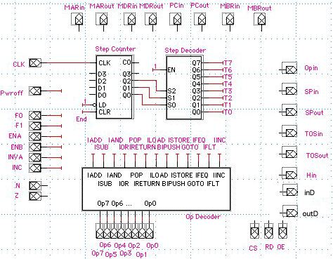
Here, the additonal devices Op Decoder, Step Counter, and Step
Decoder are also provided. The Op Decoder is a specialized
decoder that interprets each of the 13 MINIJVM op codes and sets the
appropriate switch to 1 (e.g., if Op0-Op7 = 60, then the IADD switch is
set to 1). The Step Counter is a 3-bit counter (it cycles from
000 to 111 in increments of 1), and the Step Decoder interprets these 3
bits by turning on one of the signals T0-T7 appropriately. The
CPU clock (CLK) drives this entire process.
Your task is to complete this circuit and package it as a single
device. That device should have the same shape and pin
configuration as the one that appears in the circuit Decoder Test.cct (available on the
csci220 server). However the internal circuit that's in that
device should be replaced by the one you design, based on the above
skeleton.
You may also use Decoder Test.cct
to check that your completed decoder correctly implements the fetch/execute
cycles of each of the 13 instructions in the MINIJVM instruction
set. Notice that the hex heyboard on the bottom of that circuit
can be set to each different op code (e.g., 60 = IADD) and then run to
see if the four fetch-execute steps of that instruction actually set
the right switches at the right time (e.g., T0-T4).
Part 4. Completing this Lab
Each team should turn in the following:
A. A set of answers to the questions you answered in Part 1.
B. A complete set of function definitions for each of the output
pins on the Instruction Decoder.
C. A complete Instruction
Decoder device, fully tested and submitted in your library teamAlib or teamBlib.