
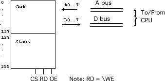
All registers shown here are 8-bit (1-byte) registers. Registers PC and MBR contain the address and value of the instruction currently being executed, while registers MAR and MDR contain the address and value of an operand of the instruction currently being executed. Register H is an intermediate register that is useful for various arithmetic operations.
![]()
Here, Op identifies the 8-bit operation code for one of these instructions. When writing an assembly language instruction like
IADD
The interpretation of IADD is that the top two bytes on the stack are popped and added, and this sum is pushed on top of the stack in their place. All numeric data in this machine is stored as 8-bit 2's complement integers. Here is a summary of the 1-byte instructions and their meaning.
Meaning (Clock cycles):The notation x = y means "assign the value of y to x" (as in Java or C), the notation "x; y" means "do x and y in the same clock cycle," and the notation "x, y" means do x and then y in two separate clock cycles." Also, "rd" means "do a memory read" and "wr" means "do a memory write." Finally, the notation "x=y=z" is like an ordinary assignment, evaluated from right to left.
Symbol Op(Hex) T1 T2 T3 T4
------ ---- ----------- --------- ------------- -------
IADD 60 MAR=SP=SP-1 H=TOS; rd MDR=TOS=MDR+H wr; End
ISUB 64 MAR=SP=SP-1 H=TOS; rd MDR=TOS=MDR-H wr; End
IAND 7E MAR=SP=SP-1 H=TOS; rd MDR=TOS=MDR&&H wr; End
IOR 80 MAR=SP=SP-1 H=TOS; rd MDR=TOS=MDR||H wr; End
POP 57 MAR=SP=SP-1 rd TOS=MDR; End
IRETURN AC Pwroff
![]()
Here is a summary of the 2-byte instructions and their meanings.
Meaning (Clock cycles):At the beginning of execution for each of these 13 instruction types, a single clock cycle, T0, fetches the instruction and then branches to one of the above sequences. It's definition is:
Symbol Op T1 T2 T3 T4 T5 T6
---------------------------------------------------------------------------------------
ILOAD 15 PC=PC+1; fetch MAR=MBR rd TOS=MDR MAR=SP=SP+1 wr; End
BIPUSH 10 PC=PC+1; fetch MDR=TOS=MBR MAR=SP=SP+1 wr; End
ISTORE 36 PC=PC+1; fetch MAR=MBR MDR=TOS MAR=SP=SP-1; wr rd TOS=MDR; End
GOTO A7 PC=PC+1; fetch PC=MBR
IFEQ 99 PC=PC+1; fetch TOS = TOS Z->PC=MBR-1 MAR=SP=SP-1 rd TOS=MDR; End
IFLT 9B PC=PC+1; fetch TOS = TOS, N->PC=MBR-1 MAR=SP=SP-1 rd TOS=MDR; End
IINC 84 PC=PC+1; fetch MAR=MBR rd MDR=MDR+1 wr; End
The IJVM has no multiplication (IMUL) instruction, so we need to rewrite our loop multiplication:f = 1;
for (int i=2; i<=n; i++)
f = f * i;
The IJVM has no for statements either, so we need to rewrite it again, this time without for loops. Also, we're dropping the declarator 'int' and the semicolon, since they're redundant at this level.f = 1;
for (int i=2; i<=n; i++) {
int s = 0;
for (int j=1; j<=i; j++)
s = s + f;
f = s;
}
f = 1At the end of this program, when control reaches the statement 'done2', the variable f will have the desired result. When generating machine language, we know that each line of the Java source program will occupy several lines of code. A comment in the middle column identifies the source statements for each group of code statements. The memory address of each code statement is in the left-hand column, and the machine code is on the right. Local variables and their addresses are listed at the bottom of the program.
i = 2
loop1: if (i>n) goto done1
s = 0
j = 1
loop2: if (j>i) goto done2
s = s + f
j = j + 1
goto loop2
done2: f = s
i = i + 1
goto loop1
done1:
Symbolic Machine Actual Machine CodeNote that the hex addresses 'Address' shown on the left are for this program's instructions, once they are translated (by hand!) to machine code.
Address Instruction Comment Op Addr
------- ---------------------- ----------------- -------------------
00 BIPUSH 1 f = 1 10 01
02 ISTORE f 36 32
04 BIPUSH 2 i = 2 10 02
06 ISTORE i 36 34
08 loop1: ILOAD n if (i>n) 15 33
0A ILOAD i goto done1 15 34
0C ISUB 64
0D IFLT done1 9B 30
0F BIPUSH 0 s = 0 10 00
11 ISTORE s 36 36
13 BIPUSH 1 j = 1 10 01
15 ISTORE j 36 35
17 loop2: ILOAD i if (j>i) 15 34
19 ILOAD j goto done2 15 35
1B ISUB 64
1C IFLT done2 9B 29
1E ILOAD s s = s + f 15 36
20 ILOAD f 15 32
22 IADD 60
23 ISTORE s 36 36
25 IINC j j = j + 1 84 35
27 GOTO loop2 A7 17
29 done2: ILOAD s f = s 15 36
2B ISTORE f 36 32
2D IINC i i = i + 1 84 34
2F GOTO loop1 A7 08
31 done1: IRETURN AC
32 f: local variables
33 n:
34 i:
35 j:
36 s: