Suppose the IJVM had no multiplication (IMUL) instruction. Then we would need to rewrite this code by simulating multiplication as repeated addition (i.e., f*i = f+f+ ... + f):f = 1;
for (int i=2; i<=n; i++)
f = f * i;
Since the IJVM has no for loops either, we need to simulate those using statement labels and if and goto statements.f = 1;
for (int i=2; i<=n; i++) {
int s = 0;
for (int j=1; j<=i; j++)
s = s + f;
f = s;
}
f = 1At the end of this program, when control reaches the statement labeled done2, the variable f will have the desired result.
i = 2
loop1: if (i>n) goto done1
s = 0
j = 1
loop2: if (j>i) goto done2
s = s + f
j = j + 1
goto loop2
done2: f = s
i = i + 1
goto loop1
done1:
          Symbolic Machine                                Actual Machine Code
 Address  Instruction                Comment		  Op Addr
 -------  ----------------------     -----------------    -------------------
  00            BIPUSH  1            f = 1                10 01
  02            ISTORE  f            			  36 32
  04            BIPUSH  2            i = 2                10 02
  06            ISTORE  i				  36 34
  08      loop1:  ILOAD n            if (i>n)             15 33
  0A            ILOAD   i               goto done1        15 34
  0C            ISUB                                      64
  0D            IFLT    done1                             9B 30
  0F            BIPUSH  0            s = 0                10 00
  11            ISTORE  s				  36 36
  13            BIPUSH  1            j = 1                10 01
  15            ISTORE  j				  36 35
  17      loop2:  ILOAD i            if (j>i)             15 34
  19            ILOAD   j               goto done2        15 35
  1B            ISUB					  64
  1C            IFLT    done2				  9B 29
  1E            ILOAD   s            s = s + f            15 36
  20            ILOAD   f                                 15 32
  22            IADD					  60
  23            ISTORE  s				  36 36
  25            IINC    j            j = j + 1		  84 35
  27            GOTO    loop2				  A7 17
  29      done2:  ILOAD s            f = s		  15 36
  2B            ISTORE  f				  36 32
  2D            IINC    i            i = i + 1		  84 34
  2F            GOTO    loop1				  A7 08
  31      done1:  IRETURN				  AC
  32      f:                               local variables
  33      n:
  34      i:
  35      j:
  36      s:
f0 = 0;
f1 = 1;
i = 2;
while (i<n) {
fn = f0 + f1;
f0 = f1;
f1 = fn;
}
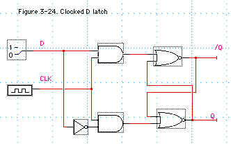
Now be sure the Fig3-24 Timing Window and Timing tool are open on your desktop. The Timing tool looks like this.
Run this simulation by sliding the above slidebar about half way to the right. Watching the signals in the Timing Window change as you switch the value of D between 0 and 1, answer the following questions.
Question 2. What is Q, and under what conditions is it on (1)? What is /Q, and when is it on? In what sense does this device represent a memory bit?
Question 3. The changes in Q and /Q do not immediately occur when there's a change in D -- that is, there's a delay. Why does this happen?
Question 4. Notice in this circuit that Q only changes on the rising edge of the clock. Modify the circuit of Figure 3-24 so that it a change in Q occurs on the falling edge of the clock, rather than the rising edge. You need not design this circuit in LogicWorks; just draw it on a sheet of paper.
You may refer to the LogicWorks Tutorial on Digital Simulation(pages 74-84) to learn more about timing and digital simulation.)
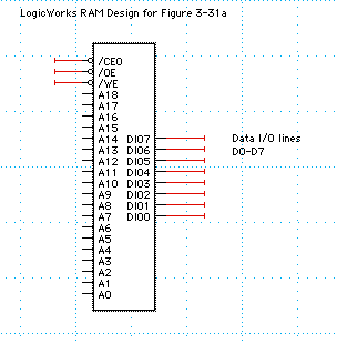
Notice that the controls /CEO and DIO0-7 are called /CS and D0-7 in Figure
3-31a. Otherwise, the two are functionally identical: there are 19
address lines and 8 data lines, so that any one of 219 = 512K separate
8-bit bytes can be read or written in a single memory operation. The
DIO lines are tri-state, in the sense that each one can hold the value
0, 1, or Z (high impedance, or "disabled") on a memory read.
You may also exercise a memory chip by attaching binary switches to the three control lines, hex(adecimal) keyboards to each group of four input address lines (A), and hex displays, tri-state buffers, and hex keyboards to the data lines (DIO). These keyboards and switches can be found in theSimulationIO.clf library.
You may construct your own custom RAM chip, such as the one you exercised in question 1. To do this, select the PROM_PLA_RAM item in the Tools menu. In the dialogue box that appears, select RAM, and the following dialog box will appear. It is already filled in so that it defines the RAM chip shown above.
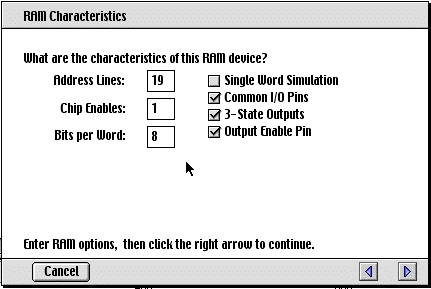
The choices here allow you to specify the number of address lines (and hence the address space) on the chip, how many "chip enable" (/CE) controls it will have, and how many bits (and hence how many data lines DIO) there will be for each addressable word. The above chip is called "byte-addressable," since each byte has a unique memory address. The other three boxes checked ensure that the same data lines are used for both read and write, and that there will be an output enable (/OE) control on the chip. Other optional settings of these boxes are not directly interesting.
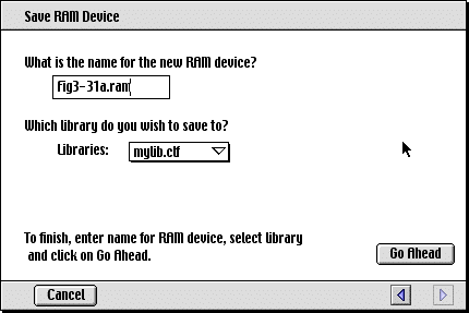
When finished, a newly-designed RAM device can be stored in your device
library mylib.clf, along with the other devices you have designed,
such as ALU. To save a RAM device in a library, that library must
be open in LogicWorks and you must give the RAM device a name, as indicated
in the dialogue box below.
Design a byte-addressable 16-byte RAM chip using LogicWorks, and name the chip "16x8" and save it in your own device library.
Exercise your RAM chip by attaching hex keyboards and displays to it, and then writing the value 10 (hex A) in each of the 16 bytes. Now rewrite the values of the words at the odd addresses to 5. Nowread the even-addressed words and check that their values are still 10.
Question 5. What settings of the controls (/CEO, /WE, /OE and the hex keyboards) are needed to store a new value, say D, in a specific memory address, say 7?
Question 6. What settings of these controls are needed to read the current value of a specific memory address, say C?
Question 7. What is the purpose of the tri-state buffer in between the hex displays and the hex keyboards on the DIO lines?
Question 8. Describe how a 2Mx32 memory can be designed using an array of 512Kx8 memory chips like the one shown above. That is, how many address lines are needed to address 2M 32-bit words? How many of these chips are needed for this memory design? How can these chips be arranged so that, for a given word to be addressed, exactly four of the chips are selected at any one time? (Hint: consider an arrangement like the one in Figure 3-29, where instead of a D-latch at each point, there's a 512x8 memory chip.)