Part 1 - Creating Your Own Device Library and New Parts
Follow the LogicWorks tutorial on pages 84-91 of the handout. When you have completed this, rename the library mylib.clf that you created during the tutorial as yourname.clf, where yourname is your login name. Below is some additional information, not in the tutorial, that you need to know to attach a circuit design to a part you have made and added to your library. Without an underlying circuit, of course, a part has no meaning.
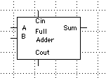
Starting with the part design that you made following the tutorial, you
should have named each of the input and output pins. For theFullAdder
part, there are three inputs (A, B, and Cin) and two outputs (Sum and Cout),
as shown below.
Now open the circuit that will be associated with this part. For
the full adder, its circuit is shown below:
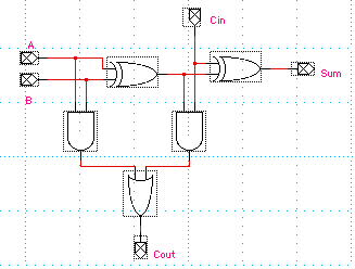
In the CONNECT.CLF library, there are connectors called "port in" and "port out". In preparation for uniting the circuit with a part, these ports are attached to the input and output wires in that circuit. The ports are given names identical with those of the input and output pins in your part design. In this step, be careful to name the ports themselves, and not the wires they are connected to. For the full adder shown below, note that the input ports are named A, B, and Cin, and the output ports are named Sum and Cout.
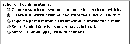
Keeping this window open, return to the device editor where your part design appears and select the DevEdit -> Subcircuit & Part Typemenu item. In this dialog box (shown below), select the second button option. This will unite the part that you created with the circuit shown above by matching the part's pin names with the circuit's port names.
Be sure to name and save this completed device in the library mylib.clf
by selecting the File -> Save Part As... menu item from the device
editor. The example developed above is named FullAdder in
the library mylib.clf on the CS220 (Tucker) server.
Check it out.
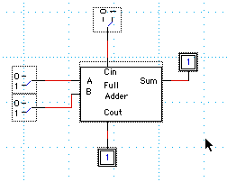
Finally, test this new part by dragging it from the library mylib.clf to a new circuit design window, attaching probes and switches in the usual way, and making sure that it gives the right output for each different input combination. This is shown below for the new part FullAdder.
Part 2 - Design an ALU (this part should be done in teams)
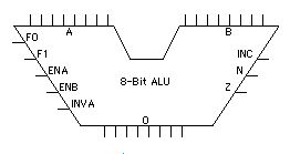
The goal here is to design a complete 8-bit ALU with the functionality
suggested in Figures 3.19, 3.20, 4.1, and 4.2. A picture of this ALU
is shown below:
This design requires several steps, and so forming teams will be useful. The work should be divided equitably among team members, so that each member has a stake in the result. Here are the teams:
Team Members
A Phillippe,
Vic, Elliott
B Brendan, Henry, Christine
First, the FullAdder you tested in the first part of this lab should be copied from mylib.clf to a new library that you create called yourteam.clf, where yourteam is A or B. Before copying, you should open both libraries in LogicWorks and use the File -> Libraries -> Lib Maint menu item.
Second, design a 1-bit ALU circuit using the guidance of Figure 3.19, but attaching a copy of the FullAdder part where it is indicated in the figure. Call this device 1BitALU and add it to the device library yourteam.clf. Identify the team member who created this device as a comment on its circuit diagram.
Third, and finally, design an 8-bit ALU out of 8 1BitALUs, using the design guidance of Figure 3.20, 4.1, and 4.2 (and the above picture). Its inputs should be F0, F1, INVA, ENA, ENB, INC, A0-A7, and B0-B7 (from right to left). Its outputs should be N, Z, and O0-O7 (again from right to left). N indicates a negative result and Z indicates a zero result (00000000). The shape of this part should be similar to that of the ALU shown in Figure 4.1 (page 205). Call this part ALU and add it to the library yourteam.clf. Identify the team member who created this device as a comment on its circuit diagram.
Be sure to test the circuits for each of these devices before you package them, so that you know they give correct output for every input. When you are done, label this device ALU and add it to the device library yourteam.clf.
2. Suggest how your ALU can be refined so that it gives an additional output V, which is 1 whenever overflow occurs on addition. Show what this additional circuitry looks like, using the names of input and output signals that are defined for ALU in Part 2.
3. When A and B represent 2s complement integers, the function A<B can be computed simply with a circuit that uses your ALU. Show how this can be done.
4. Answer questions 12, 14, 15, 17, and 18 on page 201, and 1ac, 2ac, and 5 on page 650 of your text.